873
FREE
circuits!
FREE
circuits!
How to build Frequency Doubler with 4011
August 8, 2010 - category: DigitalDescription
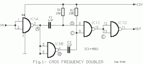
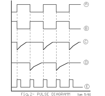
This frequency doubler uses one CMOS quad, two input NAND gate package type 4011. The frequency doubler proper consists of an inverter IC1B, two differentiating networks R1/C1, R2/C2 and NAND gate IC1A, IC1C and IC1D function as input and output buffers. In Fig.2 exist the pulses in different points of circuit.
Circuit diagrams
circuit from http://users.otenet.gr/~athsam/frequency_doubler_with_4011.htm


 This category